We describe a general synthesis of conductive gold thin films doped with entrapped organic molecules,
and demonstrate, for the first time, the immobilization of a redox couple within an electrode in a single
step. The resulting film is of dual properties: conductivity arising from the gold, and redox behavior
originating from the entrapped molecule. Faster electron-transfer rates are found for the entrapped
case, compared to adsorption. The conductivity of the film affects the organic molecule–metal interactions,
as seen in resistivity measurements, in Raman spectroscopy of the metal-entrapped molecules and from
a remarkable red shift of 30 nm in emission spectroscopy. Doping is found to affect the work function
of gold. Thin conductive doped metal films are of relevance to a variety of applications such as
electrochemical detectors, electrode materials for electrochemical impedance spectroscopy, micro and
nano electronics interconnects for packaging and for printed circuit boards. The ability to fine-tune the
work function opens the possibility to design the desired energy level gaps for optoelectronic applications
such as light emitting diodes (LEDs), solar cells and transistors.
 conductive_molecularly_doped_gold_films.pdf
 conductive_molecularly_doped_gold_films.png
In recent years, hybrid organic–inorganic perovskite light absorbers have attracted much
attention in the field of solar cells due to their optoelectronic characteristics that enable high power
conversion efficiencies. Perovskite-based solar cells’ efficiency has increased dramatically from
3.8% to more than 20% in just a few years, making them a promising low-cost alternative for
photovoltaic applications. The deposition of perovskite into a mesoporous metal oxide is an
influential factor affecting solar cell performance. Full coverage and pore filling into the porous metal
oxide are important issues in the fabrication of highly-efficient mesoporous perovskite solar cells.
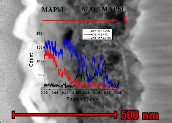
In this work, we carry out a structural and quantitative investigation of CH3NH3PbI3 pore filling
deposited via sequential two-step deposition into two different mesoporous metal oxides—TiO2
and Al2O3. We avoid using a hole conductor in the perovskite solar cells studied in this work to
eliminate undesirable end results. Filling oxide pores with perovskite was characterized by Energy
Dispersive X-ray Spectroscopy (EDS) in Transmission Electron Microscopy (TEM) on cross-sectional
focused ion beam (FIB) lamellae. Complete pore filling of CH3NH3PbI3 perovskite into the metal
oxide pores was observed down to X-depth, showing the presence of Pb and I inside the pores.
The observations reported in this work are particularly important for mesoporous Al2O3 perovskite
solar cells, as pore filling is essential for the operation of this solar cell structure. This work presents
structural and quantitative proof of complete pore filling into mesoporous perovskite-based solar
cells, substantiating their high power conversion efficiency.
Hybrid perovskite and all-inorganic perovskite have attracted much attention
in recent years owing to their successful use in the photovoltaic field.
Usually the perovskite is used in its bulk form, although recently, perovskites’
nanocrystalline form has received increased attention. Recent developments
in the evolving research field of nanomaterial-based perovskite are reviewed.
Both hybrid organic-inorganic and all-inorganic perovskite nanostructures are
discussed, as well as approaches to tune the optical properties by controlling
the size and shape of perovskite nanostructures. In addition, chemical modifications
can change the perovskite nanostructures’ band-gap, similar to their
bulk counterpart. Several applications, including light-emitting diodes, lasers,
and detectors, demonstrate the latent potential of perovskite nanostructures.
This review discusses various parameters that influence and control the organo-metal halide perovskite crystallization process. The effect of the perovskite morphology on the photovoltaic performance is a critical factor. Moreover, it has a dramatic effect on the stability of the perovskite, which has significant importance for later use of the organo-metal perovskite in assorted applications. In this review, we brought together several research investigations that describe the main parameters that significantly influence perovskite crystallization, for example, the annealing process, the precursor solvent, anti-solvent treatment, and additives to the iteite solutions.mechanisms. Control over morphology is a key parameter to understand this attractive material; morphology control will be an additional step throughout its commercialization process. The review is divided to four parts, presenting various parameters influencing perovskite crystallization and morphology. Section 2 discusses the effect of the annealing process; Section 3 describes the precursor solvent, presenting the possible solvents being used in the deposition process; Section 4 presents the anti-solvent treatment and its effect on the cell properties; and Section 5 discusses additives that can be added to the perovskite solution before deposition.
Yanqi Luo, Shany Gamliel, Sally Nijem, Sigalit Aharon, Martin Holt, Benjamin Stripe, Volker Rose, Mariana I. Bertoni, Etgar Lioz, and David P. Fenning. 8/30/2016. “
Spatially Heterogeneous Chlorine Incorporation in Organic−Inorganic Perovskite Solar Cells.” Chemistry of Materials, 2016,28, 18, Pp. 6536–6543.
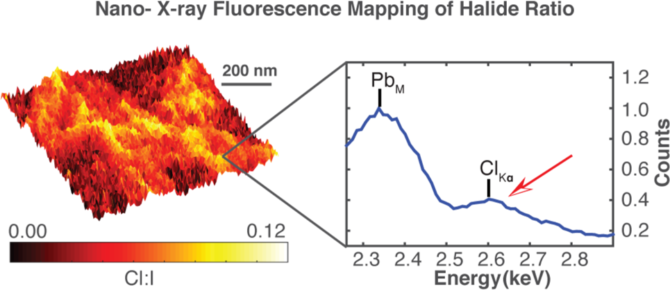
Abstract Spatial heterogeneities in the chemical makeup of thin film photovoltaic devices are pivotal in determining device efficiency. We report the in-plane spatial distribution and degree of chlorine incorporation in organic−inorganic lead halide perovskite absorbers by means of nondestructive synchrotronbased nanoprobe X-ray fluorescence. The presence of chlorine is positively identified in CH3NH3PbI3 films synthesized with Clcontaining precursors and as an impurity in some films synthesized with nominally Cl-free precursors. The impurity may be introduced from precursors or as contaminants during film synthesis. The films formed from Cl-containing precursors contain roughly an order of magnitude higher amount of chlorine, with Cl:I values greater than 0.02 found whether Cl is present in either the organic or the inorganic precursor for both one- and two-step fabrication processes. A spatial variation in the Cl incorporation is observed within single particles and as well as between particles within a given film, and the standard deviation of the Cl:I ratio across the films is up to 30% of the average
value. Understanding and controlling the heterogeneous distribution of chlorine in hybrid perovskite layers may offer a path to improve their photovoltaic performance.
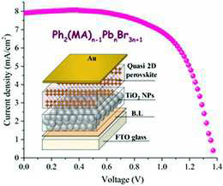
We report a hybrid mesoporous–planar architecture of methylammonium lead iodide perovskite based solar cells, to combine the benefits of both the mesoporous and planar architectures in a single device. A mesoporous-TiO2 grid was fabricated on a compact TiO2 layer, through a self-assembly process based on directional wetting, providing regions with and without mesoporous-TiO2, followed by perovskite deposition and back contact evaporation (hybrid cells). The hybrid cells showed up to 10.7% power conversion efficiency (PCE) as compared to 13.5% and 6.3% for their mesoporous and planar counterparts, respectively. Interestingly, the hybrid cells are found to show a short circuit current density
(Jsc) as high as the Jsc of the mesoporous TiO2 based cells and proved to conserve the current density even in the absence of mesoporous-TiO2 from planar parts of the hybrid cells. The cells showed the best fill factor as compared to their mesoporous and planar counterparts. The areal variation in the meso to planar ratio has also been realized by changing the grid size to demonstrate the effect of the architecture on the cell performance. Charge extraction measurements have been used to obtain insight into the recombination inside different solar cells architectures. The hybrid cell structure emerged as a novel promising design for perovskite solar cells.
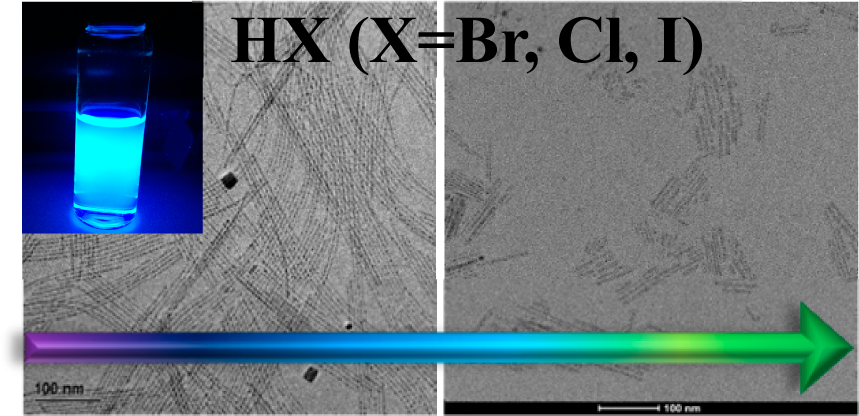
Organo-metal halide perovskite is an efficient light harvester in photovoltaic solar cells. Organometal halide perovskite is used mainly in its “bulk” form in the solar cell. Confined perovskite nanostructures could be a promising candidate for efficient optoelectronic devices, taking advantage of the superior bulk properties of organo-metal halideperovskite, as well as the nanoscale properties. In this paper, we present facile low-temperature synthesis of two-dimensional (2D) lead halide perovskite nanorods (NRs). These NRs show a shift to higher energies in the absorbance and in the photoluminescence compared to the bulk material, which supports their 2D structure. X-ray diffraction (XRD) analysis of the NRs demonstrates their 2D nature combined with the tetragonal 3D perovskite structure. In addition, by alternating the halide composition, we were able to tune the optical properties of the NRs. Fast Fourier transform, and electron diffraction show the tetragonal structure of these NRs. By varying the ligands ratio (e.g., octylammonium to oleic acid) in the synthesis, we were able to provide the formation mechanism of these novel 2D perovskite NRs. The 2D perovskite NRs are promising candidates for a variety of optoelectronic applications, such as light-emitting diodes, lasing, solar cells, and sensors.
High time resolution broadband pump-probe experiments on CH3NH3PbI3 and CH3NH3PbBr3 films are described. The improved time resolution delineates instantaneous and delayed relaxation related effects on sample absorption and assists in clarifying controversial assignment of the underlying mechanisms. Analysis of the data in terms of finite difference spectra and spectral band integrals reveals that photoexcitation is high in the inter-band continuum leading to partial bleaching and red-shifts of the exciton band just below the absorption-edge instantaneously. Increased pump intensity saturates the exciton bleach and progressively reduces inter-band absorption in a broad range extending from the band edge to higher photon energies. Both effects are attributed to reduced Coulomb enhancement due to hot carrier screening. The spectral extent of the inter-band absorption attenuation provides estimated binding energies in the range of 20–30 meV in both materials. Sub-picosecond carrier cooling reverses the initial exciton transition red-shift and induces transmission near the band edge due to state filling and stimulated emission. Finally, 1–100 ps signals are dominated by reverse state filling due to non-geminate recombination. These results demonstrate that both inter-band and exciton absorptions are essential for unraveling photo-induced dynamics in these materials, and that insights obtained from many-body theoretical analysis of dynamic screening are essential for correctly assigning the recorded spectral evolution.
In this work we study the kinetics of cesium lead halide perovskite nanoparticle (NP) growth; the focusing and de-focusing of the NP size distribution. Cesium lead halide perovskite NPs are considered to be attractive materials for optoelectronic applications. Understanding the kinetics of the formation of these all-inorganic perovskite NPs is critical for reproducibly and reliably generating large amounts of uniformly sized NPs. Here we investigate different growth durations for CsPbI3 and CsPbBr3 NPs, tracking their growth by high-resolution transmission electron microscopy and size distribution analysis. As a result, we are able to provide a detailed model for the kinetics of their growth. It was observed that the CsPbI3 NPs exhibit focusing of the size distribution in the first 20 seconds of growth, followed by de-focusing over longer growth durations, while the CsPbBr3 NPs show de-focusing of the size distribution starting from the beginning of the growth. The monomer concentration is depleted faster in the case of CsPbBr3 than in the case of CsPbI3, due to faster diffusion of the monomers, which increases the critical radius and results in de-focusing of the population. Accordingly, focusing is not observed within 40 seconds of growth in the case of CsPbBr3. This study provides important knowledge on how to achieve a narrow size distribution of cesium lead halide perovskite NPs when generating large amounts of these promising, highly luminescent NPs.